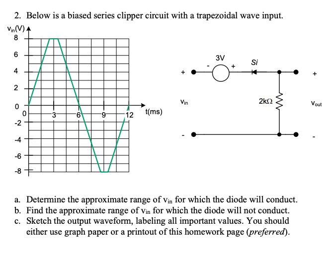
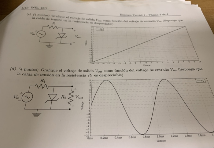
Vout Vs Vin Graph
Solved Sketch A Graph Of V Out Vs Vin And Vout Vs Vin F Chegg Com

Performance Curve Vout Vin Versus Frequency Of Low Pass Frequency Download Scientific Diagram

Dc Response Dc Response Vout Vs Vin For A Gate Ex Inverter Ppt Video Online Download
Solved The Circuit Below Has Variable Voltage Vin As Its Chegg Com
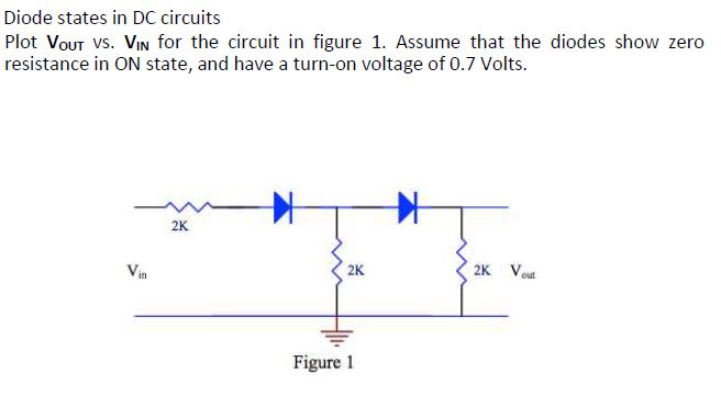
Solved Diode States In Dc Circuits Plot Vout Vs Vin For Chegg Com
Http People Ee Duke Edu Krish Teaching Lectures Addendum Sept16 Pdf
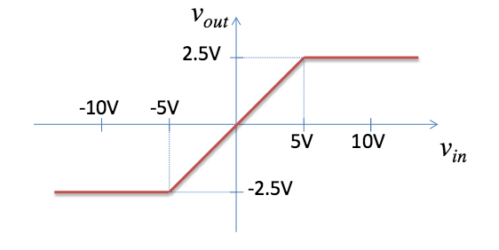
Vin for the operational amplifier circuit note that the output voltage saturates at 15 as 15 as a real operational amplifier should and as you verified in lab 5.
Vout vs vin graph. Set 10 you were to generate i v graphs for both nmos and pmos devices. You can draw a point on the graph at vin 2v and vout 2v. Transfer curve vout versus vin for a cmos inverter. Find vout f vin voltage transfer characteristic vtc plot of vout as a function of vin vary vin from 0 to vdd find vout at each value of vin.
Vin is an energy source and will always be drawn to a vout because most often your vout will be a ground. Probe is a fairly versatile plotting package. Eg from 1 5v to 2 5v. Viewed 2k times 2 begingroup the graphic is in log vout vin vs log f.
A vin and vout identify the direction of electron flow in your electrical circuit. I think that for. So you can add a straight line to the graph showing vout vin over that range. You in the left column vin and vout were relatively easy to find.
Mason lecture notes 7 2 inverter voltage transfer characteristics output high voltage v oh. You can select each axis to edit its attributes by clicking on it. Figure 16 shows the result of adding a second vertical axis. Active 4 years 10 months ago.
Ask question asked 4 years 10 months ago. No current flows through the resistor so vout vin 2v. By over laying these graphs in a sensible way you can generate the transfer curves. The resulting graph is shown above in red.
If you notice the maximum gain is located at 0db. What sort of graph of vout vin vs frequency will a low pass and high pass filters have. If you did this correctly check with the solutions you have nmos i v in quadrant 1 and pmos in quadrant 4.
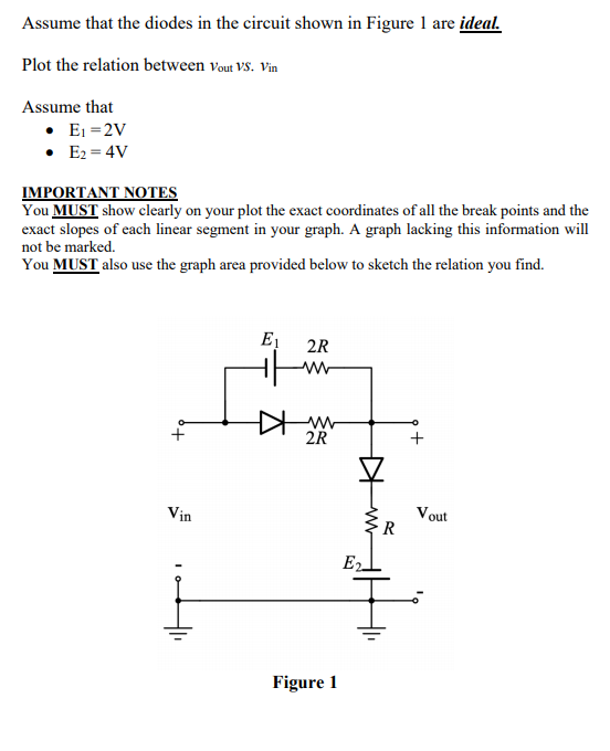
Solved Assume That The Diodes In The Circuit Shown In Fig Chegg Com
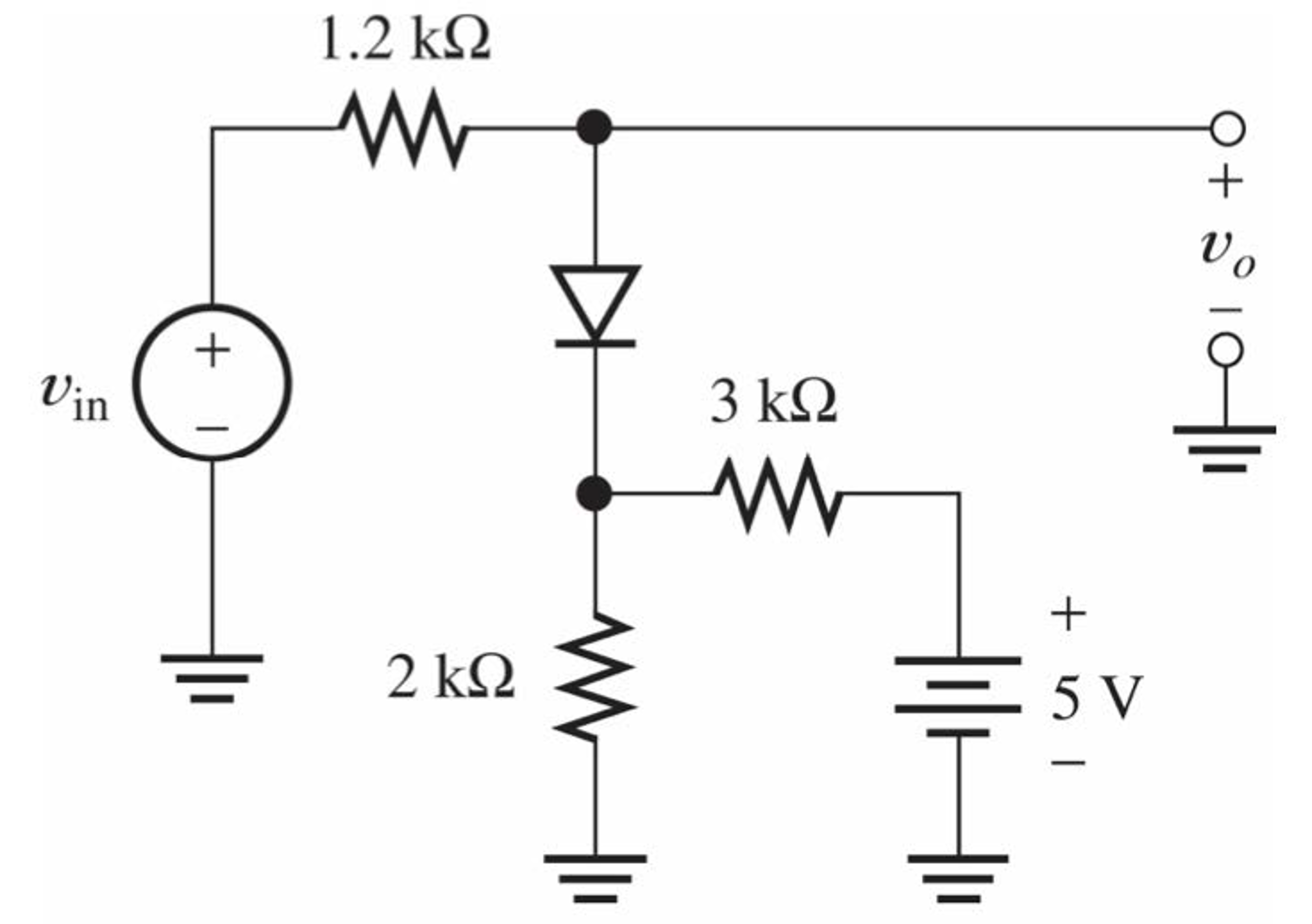
Solved Plot The Transfer Function Vout Vs Vin For The Ci Chegg Com

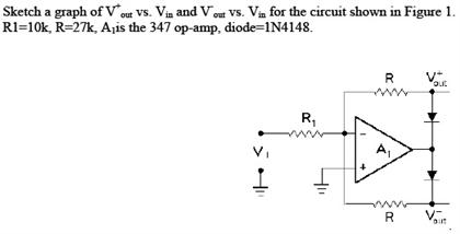
Op Amps Dp
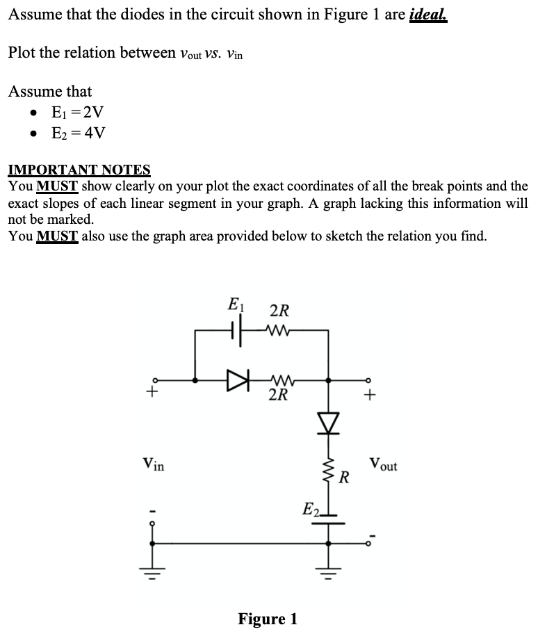
Solved Assume That The Diodes In The Circuit Shown In Fig Chegg Com

Lp2992 Ldo Operation Below Its Regulation Voltage Power Management Forum Power Management Ti E2e Support Forums

Lecture 21 Outline The Mosfet Cont D P Channel Mosfet Ppt Download

Hysteresis Of The Schmitt Trigger A Vin Vs Vout Characteristic B Download Scientific Diagram
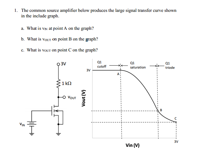
1 The Common Source Amplifier Below Produces The Chegg Com
Solved Graph Vout As A Function Of Vin C Graph The Outpu Chegg Com
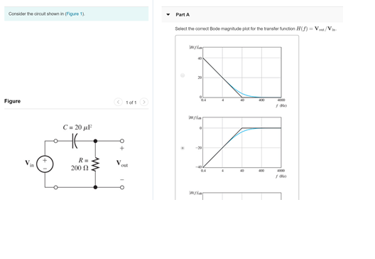
Solved Can You Please Show Me How To Find The Correct Bod Chegg Com
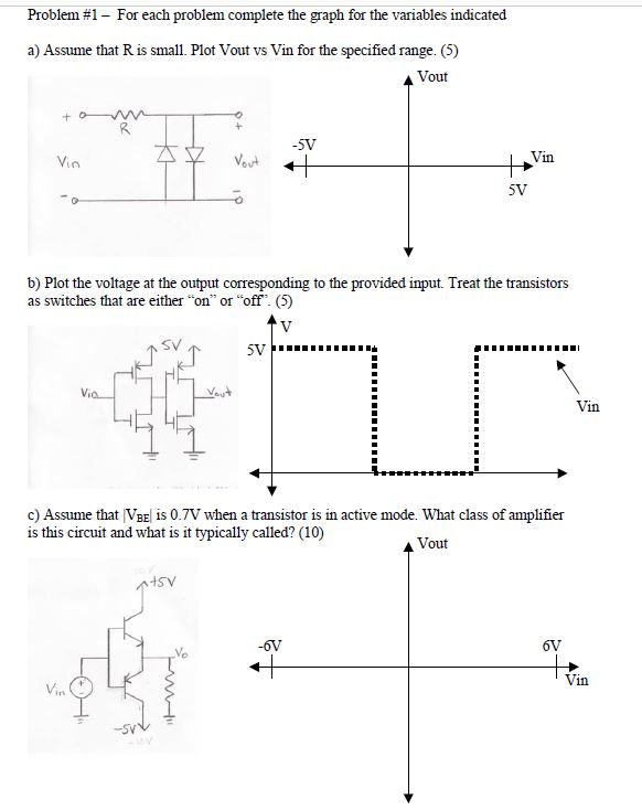
Solved Problem 1 For Each Problem Complete The Graph For Chegg Com
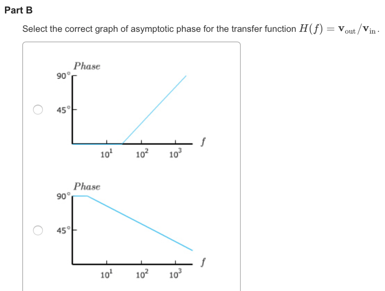
Solved P 6 10 The Transfer Function H F Vout Vin Of A Fi Chegg Com
Http Resource Download Wjec Co Uk S3 Amazonaws Com Vtc 2016 17 16 17 1 9 Gce Electronics Book Chapter 4 Pdf